
 Алгебра
 Английский
 Биология
 География
 Геометрия
 История
 Русский
 Обществознание
 Физика
 Химия
Химия Информатика
 Литература
 Математика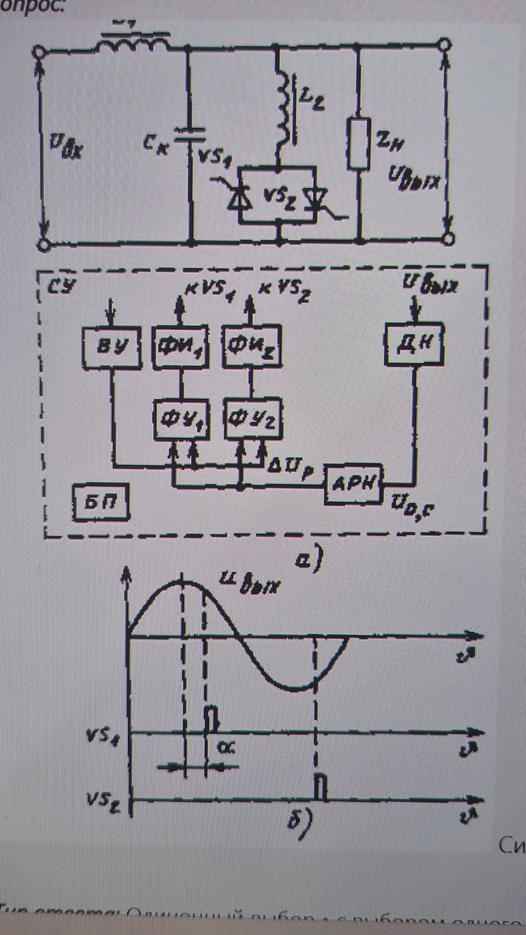
Ответ:
Analysis of the Electrical Circuit and Graphs
The provided image displays an electrical circuit diagram and two graphs (labeled \(\alpha\) and \(\delta\)), illustrating the operation of a power converter, likely a controlled rectifier or inverter system. The circuit includes an input voltage \( U_{вх} \), an inductor \( L_2 \), a capacitor \( C_K \), thyristors (switches) \( VS_1 \) and \( VS_2 \), a load \( Z_H \), and an output voltage \( U_{вых} \). A control system ( \( СУ \) ) is also depicted, which manages the firing of the thyristors.
Components and their Functions:
- \( U_{вх} \): Input voltage, likely AC or DC, which is being converted.
- \( L_2 \): Inductor. This component typically smooths current or stores energy in a switching circuit.
- \( C_K \): Capacitor. This component typically filters voltage or stores charge.
- \( VS_1, VS_2 \): These symbols represent thyristors (SCRs - Silicon Controlled Rectifiers). They are semiconductor devices that act as electronic switches, allowing current to flow in one direction when triggered by a gate pulse, and blocking current otherwise. Their conduction can be controlled by the firing angle.
- \( Z_H \): Load impedance. This represents the connected device or circuit that consumes the converted power.
- \( U_{вых} \): Output voltage delivered to the load.
- \( СУ \) (Control Unit): This block represents the control circuitry responsible for generating the firing pulses for the thyristors. It likely receives feedback signals and processes them to regulate the output. The sub-blocks \( ВУ \) (Voltage Unit), \( ФИ_1 \) and \( ФИ_2 \) (likely filters or signal conditioners), \( ФУ_1 \) and \( ФУ_2 \) (likely functional units or signal processors), \( ДН \) (Driver), \( АРН \) (Automatic Voltage Regulator), \( БП \) (Power Supply), and \( U_{p,c} \) (reference voltage or setpoint) are part of this control logic. \( \Delta U_p \) could represent a voltage difference.
Operation and Graphs:
The graphs illustrate the control strategy, likely Pulse Width Modulation (PWM) or phase control, for the thyristors \( VS_1 \) and \( VS_2 \).
- Graph \(\alpha\) (likely represents \( U_{вых} \) over time, and control signals):
- The top waveform shows a sinusoidal voltage, likely the input voltage \( U_{вх} \) or a voltage related to it.
- Below this, two waveforms represent the gate trigger pulses for \( VS_1 \) and \( VS_2 \).
- \( VS_1 \) is triggered by a pulse at a specific angle \( \alpha \) relative to the zero crossing of the input voltage. This suggests phase control, where the timing of the pulse determines the output voltage magnitude.
- \( VS_2 \) appears to be triggered by a separate pulse train, possibly for bidirectional control or in conjunction with \( VS_1 \) to achieve a desired output waveform.
- Graph \(\delta\) (likely represents control signals for another aspect of the system or a different mode):
- This graph shows distinct pulse signals for \( VS_1 \) and \( VS_2 \), occurring at different times. This might indicate a different control mode, such as a PWM strategy where pulses are applied to control the duty cycle, or a different phase angle for \( VS_2 \).
Overall Operation:
The circuit likely operates as a controlled AC-to-DC converter or an AC-to-AC converter (like a cycloconverter or phase controller). The control system \( СУ \) monitors the output voltage and compares it to a reference \( U_{p,c} \). Based on the difference \( \Delta U_p \), it adjusts the firing angles \( \alpha \) (and potentially other parameters) of the thyristors \( VS_1 \) and \( VS_2 \) to maintain the desired output voltage \( U_{вых} \) across the load \( Z_H \). The inductor and capacitor likely play roles in filtering and energy storage to ensure a stable and controlled output.
